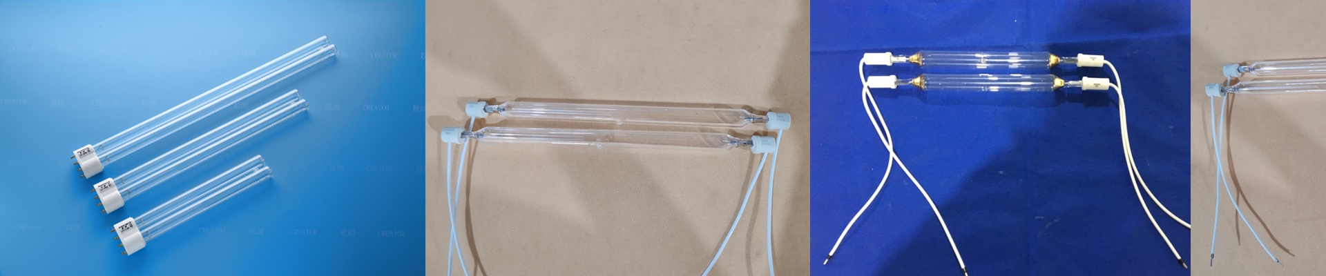

Out on the PCB floor, the solder mask cure is where the micron-level tolerances meet the reality of photopolymerization. Fine lines, tight clearances, dense vias—there’s zero room for under-cure. When cross-linking isn’t complete, you see adhesion loss, brittleness, and bridging during hot air leveling. The UV lamp has to hit the board with stable, high-peak irradiance, and do it without hot spots that can warp laminates. What actually matters isn’t marketing—it’s spectral output and energy density. The SK15 UV lamp, with its ceramic base, is built around a high-pressure mercury vapor discharge that’s tuned for a strong 365 nm peak, plus enough balanced medium-wave output to fully activate the photoinitiators in solder mask inks. The ceramic base keeps thermals in check and holds electrode temperature steady, so output drift stays minimal over the life of the lamp. You get stable spectral output, a reflector geometry that lays down a uniform intensity profile, and a measured dose that clears the ink’s required mJ/cm² window. The payoff is repeatable curing across 25–50 μm line/space features, with no residual tack. Here’s why it works in this environment: PCB lines are narrow, and the substrate doesn’t like heat. The SK15’s ozone-free design and controlled spectral profile let you cure at line speed without scorching FR-4 or delaminating thin copper. That translates to consistent adhesion, less rework, and predictable lamp life. And if you’re running offset, flexo, or screen platforms, the SK15 can be matched to the process. Need higher peak irradiance for thicker screen deposits? Done. A slightly broader spectral output for flexo films? Set it up. Tight focus for offset films? You can get there—without changing the curing chemistry. A few practical notes. Match the lamp to your curing station’s arc length and reflector focal distance. Verify power supply compatibility—voltage and ignition method—and make sure the dichroic coating lines up with your spectral window. Keep a radiometer on output, and plan lamp replacement when intensity drops below your process window. Depending on duty cycle, that’s typically 5,000–8,000 hours. Double-check the SK15 dimensions and connector type against your holder. A mismatch can mean poor contact and unstable ignition, and you don’t need either on the line.
在PCB生产车间,焊锡防焊层固化是微米级公差与光聚合现实交汇的关键工序。细线、紧密间距、密集过孔——对固化不足没有任何容忍空间。当交联不完全时,会出现附着力下降、脆化以及热风整平时的桥连现象。紫外灯必须以稳定且高峰值的辐照强度照射电路板,且不能产生可能导致层压板翘曲的热点。
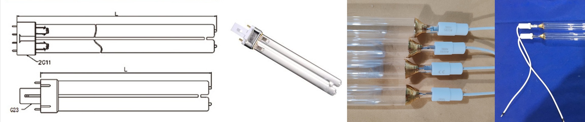
真正关键的不是市场宣传,而是光谱输出和能量密度。SK15紫外灯采用陶瓷基座,基于高压水银蒸气放电设计,调谐出强烈的365 nm峰值,同时具备足够均衡的中波段输出,能完全激活防焊油墨中的光引发剂。陶瓷基座有效控制热量,保持电极温度稳定,使灯具使用寿命内输出漂移最小。
您将获得稳定的光谱输出和反射器几何形状,确保光强分布均匀,并且剂量测量满足油墨所需的mJ/cm²范围。结果是在25–50 μm线宽/间距特征上实现可重复的固化,且无残留粘性。
其适用性的原因在于:PCB线路细窄,基板对热敏感。SK15的无臭氧设计和受控光谱特性允许在线速度下固化,避免烧焦FR-4材料或使薄铜层分层。这带来稳定的附着力、减少返工以及可预测的灯具寿命。
如果您使用胶印、柔版或丝网印刷平台,SK15可以根据工艺进行匹配。需要更高峰值辐照度以固化较厚的丝网印刷层?可以实现。需要稍宽光谱输出以适应柔版薄膜?可以调整。需要紧凑聚焦以适配胶印薄膜?也能实现——无须更改固化化学体系。
几个实用建议。请将灯具与固化站的电弧长度及反射器焦距匹配。确认电源兼容性——电压和点火方式是否匹配,并确保二色膜涂层与您的光谱窗口对齐。使用辐射计监控输出,并在强度低于工艺要求时安排更换。视工作周期,一般寿命为5,000–8,000小时。
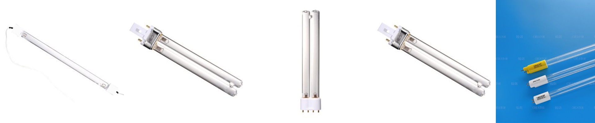
务必再次核对SK15的尺寸和连接器类型是否与灯座匹配。若不匹配,可能导致接触不良和点火不稳定,这两者在线上都不可接受。